
2J2 Understand the function of stabilising circuits and identify different types of stabilising circuits (i.e. Zener diode/pass transistor and IC).
Note: questions on the characteristics of individual components are covered earlier in this syllabus, e.g. This sub-section is on complete circuits.
The Regulation must be able :-
The other part that is needed is some form of REGULATOR to keep the output voltage at say 13.8V all the time without any regard as to the level of current being drawn.
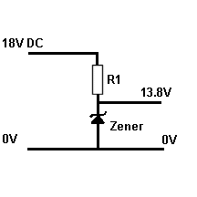
In its simplest form, for low current use, a regulator could be as simple as a Zener diode and a resistor in series across the DC supply. The value of the zener diode determines what the output voltage is.
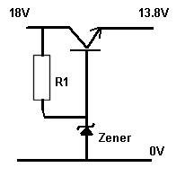
The next stage would be to add a pass transistor as shown below. Here again the zener determines the output voltage.
The next stage in complexity would have a regulator which consists of a few more components as shown in the diagram below as it develops. In this case it is the variable resistor as part of the potential divider chain of resistors that determines the output and thus can be "set" to the output required.

The transistor at the top is called a PASS TRANSISTOR as it is passing all the current going to the output terminal. The lower transistor is part of the regulator circuit. Please note a ZENER diode has been used at a voltage of 5.6V. Such a rated diode performs very well and can control the voltage close to 5.6V without change due to heating.
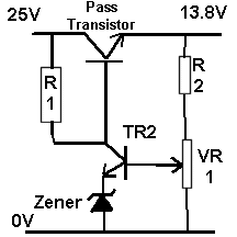
With the power turned on the preceding part of the circuit will supply 25V to the collector of the pass transistor. R1 will then supply a small current to the base of the pass transistor and current will then flow through the transistor to the output terminal where the diagram is marked 13.8V.
-------------------------
The 13.8V is controlled by the potential divider chain of R2 and VR1 which controls the current flowing into the base of the second transistor. If the 13.8 goes higher then more current flows into the base turning TR2 on harder. This results in there being less current available to the base of the pass transistor, hence the output falls to a point where there is equilibrium in the circuit. The zener is always conducting, providing a reference voltage against which the output voltage is compared. If the 13.8V goes lower then less current flows into the base and TR2 begins to turn off. This results in there being more current available to the base of the pass transistor, turning it on more, and the output voltage rises to the point where again there is equilibrium in the circuit.

This action continues and thus regulates the output voltage and stabilizes it to 13.8V +/- a very little. VR1 is used to set the output level at 13.8V initially.
The use of an IC
It is possible to carry out many of the above functions with an IC such as LM723 which is a voltage controlling IC. Discussion in the course is not required other than to be aware that IC's can control voltage circuits of a power a supply when used in conjunction with pass transistors and other components.
2J3 Understand the need for rectifier diodes to have a sufficient peak inverse voltage (PIV) rating and be able to calculate the PIV in diode/capacitor circuits.
2J4 Understand the basic principles and operation of a switch mode power supply, at block diagram level
The block diagram concept was introduced to you at Foundation Level as it only shows the blocks of parts which make up the whole unit and does not go to component level.
A Switch Mode Power Supply (SMPS) is a type of power supply that uses switching devices (typically transistors) to convert electrical power efficiently. The key feature of SMPS is its use of high-frequency switching to convert input power to the desired output voltage and current.
Key Components of an SMPS:-
Input (AC or DC): The SMPS can take either an AC or a DC input usually preceded by an EMI/EMC filter. In AC-to-DC applications, an AC voltage is first rectified into DC.
Rectifier (if AC input): Converts the AC input voltage into DC. This is typically done using diodes or a bridge rectifier.
Control Circuit:
This circuit manages the operation of the switch. It determines the duty cycle and timing for the switching device (like a transistor or MOSFET). The control circuit uses feedback to maintain a constant output voltage or current, compensating for variations in the input or load.
The feedback can come from different sources, such as voltage feedback, current feedback, or a combination of both.
Power Switch:
The power switch is typically a transistor or MOSFET that rapidly switches the input power on and off.
The frequency of the switch is usually very high (in the range of tens to hundreds of kHz), which allows the use of smaller passive components (inductors and capacitors) for filtering.
Inductor (Energy Storage):
The inductor stores energy during the "on" period of the switch and releases it during the "off" period.
It smooths out the current delivered to the load by preventing large fluctuations.
Filter Capacitor:
A capacitor is placed at the output to smooth out the voltage ripple caused by the switching action. It reduces noise and helps maintain a stable output voltage.
Output:
The final output voltage and current, which can be either DC or regulated AC, depending on the design of the SMPS.
How It Works:
Rectification (if AC input):
In case of an AC input, the first stage is rectification, converting AC voltage to DC.
If the input is already DC, this stage is skipped.
Switching Action:
The control circuit regulates the power switch (MOSFET, transistor, etc.) to switch at a high frequency.
The duration the switch stays on (duty cycle) is controlled to regulate the output voltage or current.
The power switch operates at high efficiency because it is either fully on or fully off, minimizing energy loss.
Energy Transfer:
When the switch is "on," current flows through the inductor, which stores energy.
When the switch is "off," the inductor releases its stored energy to the load.
Filtering:
After the energy is transferred, the inductor and capacitor smooth the output signal, reducing ripple and providing a stable DC output.
Feedback:
A feedback mechanism continuously monitors the output voltage or current.
If the output deviates from the desired value, the control circuit adjusts the duty cycle of the switch to correct it.
Advantages of SMPS:-
High Efficiency: The use of switching transistors in a fully "on" or "off" state reduces losses, leading to higher efficiency compared to linear power supplies.
Smaller Size: Due to the high switching frequency, the passive components (such as inductors and capacitors) can be much smaller.
Versatility: SMPS can be designed to output various voltages (both step-up or step-down) and are used in a wide range of applications.
In summary, an SMPS efficiently converts power by switching the input on and off rapidly, storing energy in inductors, and filtering it to provide a stable output. The high-frequency switching allows the design of smaller and more efficient power supplies.
Review and more Summary
The mains supply enters an "Input Filter" which takes out any spurious electrical noise which may be generated in the power supply from going back in to your mains supply in your property. Such a filter is present in a good quality switch mode power supply.
The mains AC voltage is fed into a "Rectifier Circuit" to provide High Voltage DC, and as in a traditional power supply with a transformer there will normally be a reservoir capacitor following the rectification.
The next part is a "Chop" comprising of high voltage transistors acting as switches on and off, which chops up the DC into short pulses at around 30 to 60 kHz. As these transistors are either on or off, the power dissipation is low compared to the traditional power supply switching transistors.
The pulses are then fed into a "Transformer" which converts the high voltage pulses to pulses of the required voltage, which it passes to the next stage. As the transformer is dealing with relatively high frequencies compared to the usual 50Hz supply, the transformer in a Switch Mode Power Supply can be much reduced in size. Also the Transformer has a Ferrite Core and not a Soft Iron so that the core does not become "saturated" and stop working. The winding of the transformer are also well insulated.
After the Transformer stage is another "Rectifying Circuit" which converts the High Voltage DC to Low Voltage DC. The regulation of the DC pulses to the required voltage is achieved by looking at (or in electrical terms "Sampling") the output voltage of the pulses, and comparing the pulses via an opto-isolator (also know as an opto-coupler), to control "The CHOP" of the pulses' width on the primary side of the transformer.
A smoothing capacity will exist after the second rectification block diagram and this capacitor can be much smaller than in the conventional power supply because it is working at higher frequency of about 50kHz.
Making sure the OUTPUT voltage is as required there is a feed back circuit through an opto coupler which acts to isolate the signal but passes the pulse width to the primary side of the transformer.
Whilst the whole unit is much smaller than the conventional power supply it does have a down side, it can create harmonics due to the switching.
The "Input filter" stops the harmonics leaking back into the mains supply and an other "Output Filter" ensures that no harmonics go into the low voltage supply to your equipment.
Such filters are present in a good quality switch mode power supply. Failure to have good filtering and screening can create high background RF noise which would be picked up on your radio receiver.
Here is a picture of a typical Switch Mode Power Supply

Terminals marked L and N are the mains input terminals V+ and V- are the DC output connections.
The origin of some of the text on this page is from the RSGB with additions by the web master