

Technical Basics
Semiconductor devices - Transistors
2I3 Understand that a bipolar junction transistor is a three terminal device (emitter, base, collector) in which a small base current will control a larger collector current and this enables the transistor to be used as an amplifier.
Before we go into the syllabus fully we must take moment to describe what a transistor is and it basic operation.
The circuit diagram of an NPN transistor is:-
![]()
We previously discussed the PN junction when we where looking at diodes.
The transistor is called a Bipolar transistor it has 2 junctions and 3 separate connections.
The transistor has a thin layer of P type material sandwiched between 2 thicker N type layers hence the name NPN transistor or bipolar transistor.
![]()
The layer which forms the middle of the sandwich is called the BASE, the others are called EMITTER and COLLECTOR respectively.
![]() The arrowhead points in the conventional
direction of current flow.
The arrowhead points in the conventional
direction of current flow.
The transistor like the diode needs forward bias to turn the transistor on and then the main current will flow through the transistor from the collector to emitter.
Summary
Bipolar transistors
-
Bipolar transistors consist of three regions - EMITTER, BASE, COLLECTOR, - with 2 junctions.
-
Current flows between collector and emitter only when current flows between base and emitter.
-
A transistor has GAIN when collector current divided by the base current is greater than 1.
-
Connecting transistors in different ways changes gain and input/output impedances.
FIELD EFFECT TRANSISTORS.
To be strictly correct, the so-called FIELD EFFECT TRANSISTOR is not a transistor at all, as the word TRANSISTOR is derived from TRANSFER RESISTOR and the FET doesn't work like that at all. The FET relies upon the prescence and the effects of an electric field
There are 2 types of FET - The JUNCTION FET and the METAL OXIDE SILICON FET or MOSFET.
Both work by controlling the flow of current carriers in a narrow channel of silicon. The main difference between them lies in the way the flow is controlled.
Firstly the JUNCTION FET. A tiny bar of N or P type silicon has a junction formed near to one end. Connections are formed at either end of the silicon bar (see drawing) and also to the junction material (p type for N type FET).
The P type connection is called the GATE, the end of the bar nearest the gate is called the SOURCE, and the connection at the other end is called the DRAIN.
A junction FET is normally used with the junction reverse biased (it has a negative voltage on it for an N channel as opposed to what you might expect a positive one) so that a few moving carriers are around the junction (keeping it turned off) making the bar of silicon itself a poor conductor.
With less reverse bias (or less negative volts) on the junction the silicon bar will conduct better, and so on as the amount of reverse bias on the junction decreases the FET conducts better.
When a VOLTAGE is connected across the SOURCE and DRAIN the amount of current flowing between them depends on the amount of reverse bias (or negative volts) on the GATE and the ratio SOURCE - DRAIN CURRENT/GATE VOLTAGE is called the MUTUAL CONDUCTANCE the symbol for which is Gm. This quantity is a measure of the effectiveness of the FET as an amplifier of current flow.
Because the GATE is REVERSE BIASED, practically NO GATE CURRENT FLOWS, so that the RESISTANCE between GATE and SOURCE is VERY HIGH, much HIGHER than a BASE EMITTER junction of a BIPOLAR transistor, This uncommonly high resistance is put to good use, for instance in voltage measuring circuits NO LOAD is put on the circuit being measured.
NPN transistor used as an AUDIO amplifier
![]()
Transistor biased on by R1/R2. To compensate for changes in:
-
operating voltage (battery equipment, batteries getting tired)
-
variations in operating temperature
-
variations in transistor specifications (even from the same batch).
Then R4 is used to provide 100% negative feed feedback at DC. The reason this works, is because if the transistor takes more collector current, then this current passes through R4, and a bigger voltage would appear across it as a result. This voltage opposes the bias voltage that is set by R1/R2, and thereby stabilizes the transistor against changes as in 1) to 3) above.
Understand that the ratio of the collector current to the base current (IC/IB) is the current gain β or hFE of the transistor.
A Transistor is a current amplifying device. β is the DC current gain of a transistor in a common emitter mode PNP or NPN transistor. If the current on the base of the transistor is Ib and the collector current is Ic.
![]() = Ic / Ib
= Ic / Ib
So if the base current Ib is 10uA and the collector current Ic is 1mA :-
Beta = 1mA/10uA = 100
If a transistor has a β of 200 and the bases current Ib is 100uA then the collector current would be 200 times greater
or β x Ib = 200 x 100uA = 20mA
For a transistor to work correctly as an amplifier the correct proper potential voltage must be present on base, collector and emitter so the transistor is biased to achieved this.
Normally the term bias refers to the voltage applied to the base to bring the operating point to a linear part of the transistor amplification curve . For a Germanium transistor a voltage between emitter and base of 0.3 volts and for a silicon transistor 0.6 volts.
Understand that if the variation in the base current is
large enough the collector current can be turned on and off
and the transistor behaves as a switch.
Note: It is not required to recall transistor
configurations. Circuits shown will use an NPN transistor
connected in common emitter mode.
NPN transistor used as a switch
![]()
In this configuration when the link is made between R1 and 9V the LED turns on.
This is because the current can flow from 9v through the resistor R2 and the LED through the transistor to ground.
![]()
When the link is made between R1 and 9V the LED is turned off.
This is because the transistors turns on and makes the collector to R2 link the same potential as ground and the LED has no current flowing as it all flows through the transistor (the easier path).
Here, we are not concerned with amplification of a signal such that we want a faithful (and larger) reproduction of the signal on the output of the transistor. We need DC stability (i.e. the transistor should stay "off" when intended, and not be affected by transistor type variations, temperature, or supply voltage). We also need the transistor to turn fully "ON", again not affected by the above variations.
This is fortunately simple; we have only to ensure that there is a resistor connected between base and emitter (R3) to ensure it is held "OFF", and then apply, via a resistor (R1), some current to the base. What we apply needs to be enough to ensure that the transistor is fully turned on despite variations as above, and also be enough to allow some to go through R3, (This resistor "nicks" it from the transistor!).
The on and off concept according to the configuration.
Ask your tutor to build a small circuit based upon the above so that you can see the difference between the two circuits in that sometime applying a current to the base turns the led on and sometimes it is the other way round that applying a current turns the led off.
![]() You might like to know that the
other type of transistor is a PNP transistor has a thin layer of
N type material sandwiched between 2 thicker P type Layers. The
arrowhead on the emitter symbol distinguishes the transistor as
being either NPN or PNP.
You might like to know that the
other type of transistor is a PNP transistor has a thin layer of
N type material sandwiched between 2 thicker P type Layers. The
arrowhead on the emitter symbol distinguishes the transistor as
being either NPN or PNP.
2I4 Recognise the circuit of a simple common emitter amplifier.
As mentioned above the Common Emitter is so called as the emitter is common to both the input and the output in that with regard to signals, it is de-coupled to ground via a capacitor and both input and output have a grounded connection. The emitter resistor does have some involvement in connecting the emitter to ground, but its main function is to set the correct DC operating conditions. The output signal is an inverted, larger copy of the original.
Phase changeThere is a phase change between input and output as shown in the drawing it being 1800 out of phase.
Voltages gain - High (about 100)
Current gain - High (50 - 800)p
Input resistance Medium - (about 5k Ω>
Output resistance High - (about 40kΩ)
Calculate the value of the collector resistor to set the collector voltage midway between V supply and 0V given the base current and transistor gain β.
CURRENT GAIN hfe ( previously it was ![]() )
)
The amount of current flowing between the collector and the emitter of a BIPOLAR transistor is much greater than the current flowing between the base and the emitter, but the amount of current flowing through the collector is controlled by the amount of base current.

The diagram above shows the basic NPN transistors with connections B base C collector and E emitter. It must be understood that the Base terminal is always positive with respect to the Emitter and that the Collector supply voltage is positive with respect to the Emitter, it is hoped you can see the little + and - in the image. For a bipolar NPN transistor to conduct the Collector is always a greater positive value than both the Base and the Emitter values. With this in mind we can continue to discuss the NPN transistor.
Electrons flowing through the Base is called the base current Ib similarly flowing though the Collector is the Ic and from the Emitter a current of Ie. As you should expect there is a relationship between these three currents !! The amount of current flowing through the Emitter equals the current through the collector plus that through the base so Ie = Ic + Ib and also Ic = Ie - Ib.
Thus you should be able to see that there is a relation ship between the Collector current and the Base current and both have an effect on the Emitter current.
We now introduce a new term "current
gain" and the symbol used to indicate current gain is hfe
( which is also known as ![]() and in an exam could be either !!)
and in an exam could be either !!)
A low gain transistor might have a gain of around 20 - 50, Power transistors sometimes have a gain of only 10, a high gain transistor might have a gain of 300 - 800 or even more.
The current flowing through the collector = the hfe (or
![]() )
times the current flowing in the base.
)
times the current flowing in the base.
The equation for the calculation of gain is Ic
= hfe x Ib or
Ic = ![]() x Ib
x Ib
So in a NPN Transistor it is the movement of the "negative electrons" through the Base (the input circuit) that causes the transistor to turn on and provide the energy to cause a link between the Collector and Emitter circuit (the output circuit which could be on the emitter or collector). This link between the input and output circuits is the feature of transistor action and which causes the amplification of the input signal on the Base to the output circuit all due to the control which the Base exerts upon the Collector to Emitter current.
Tolerances of hfe/![]() values are very large, so that even
transistors of the same type or of the same batch may have
widely different gains. Published figures of
transistor gains are only typical values. If an exact gain is
wanted then the transistor will have to be tested and selected
to do the job required. The secret is not to design a circuit
where the maximum gain is required from a transistor, but to
design such that many different devices can be used for the
same circuit.
values are very large, so that even
transistors of the same type or of the same batch may have
widely different gains. Published figures of
transistor gains are only typical values. If an exact gain is
wanted then the transistor will have to be tested and selected
to do the job required. The secret is not to design a circuit
where the maximum gain is required from a transistor, but to
design such that many different devices can be used for the
same circuit.
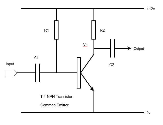
Diagram of a Common Emitter Transistor Amplifier
So to calculate the resistor value R2 in the diagram with Vc at half the supply voltage where say the transistor collector current is 1.5mA we just use our ohms law triangle where R = V/I.
In this case the Vc required is 6 volts and the current is 0.0015 Amp. So R = 6 / 0.0015 = 4000Ω or 4 KΩ.
Recall that semiconductors must be provided with the correct DC voltages and currents to allow them to function and that this is termed biasing.
For a transistor to work correctly as an amplifier the correct potential voltage must be present on base, collector and emitter so the transistor is biased to achieved this.
Normally the term bias refers to the voltage applied to the base to bring the operating point to a linear part of the transistor amplification curve . For a Germanium transistor a voltage between emitter and base of 0.3 volts and for a silicon transistor 0.6 volts.
Understand in simple terms how a (current) signal at the base causes a larger current signal at the collector and resulting change in instantaneous collector voltage.
![]()
In this diagram the transistor has slightly different biasing resistors but we do not need to understand them at this time. All we need to know that the gain β shows the amplification factor and that a small a.c. signal on the input to the base will give rise to a larger a.c signal on the collector, and N.B. it has phase shifted 180°.
2I5 Recall that a transistor can be used to generate audio and radio frequencies by maintaining the oscillations in a tuned or frequency selective circuit.
Distinguish between a crystal oscillator and a variable
frequency oscillator (VFO) based on a tuned circuit.
Diagrams will show the Colpitts oscillator with the
transistor in emitter follower mode. Candidates are not
expected to recognise other types of oscillator.
Oscillator purpose is to provide accurate and controllable waves of known frequency. To sustain oscillations feed back is required from the output to the input in a controlled way to limit the output to just a single frequency.
The above are not practical circuits as no off bias exists to the transistor BUT the important parts to recognise are those that have been highlighted.
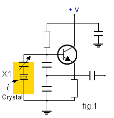
The diagram fig.1 above shows a crystal, and thus is a fixed frequency Crystal Oscillator. Do not be confused with the variable capacitor into thinking that it is a variable oscillator as the variable capacitor is there to bring the crystal oscillator to resonance at a particular frequency. sometime the variable capacitor is not even in the circuit.
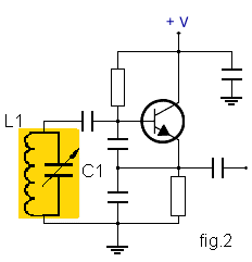
The diagram fig.2 shows a tuned circuit highlighted and also shows a variable capacitor in parallel with an inductor, making up the tuned circuit, and thus is a variable frequency oscillator.
![]() Lossy: You put some in, and don't
get it all back out! The transistor amplifier only has enough
gain to make the circuit oscillate when the coil and capacitor
are not "lossy" (i.e resonant), it oscillates at one frequency.
Lossy: You put some in, and don't
get it all back out! The transistor amplifier only has enough
gain to make the circuit oscillate when the coil and capacitor
are not "lossy" (i.e resonant), it oscillates at one frequency.
![]() Gain: The ability of the circuit to take a small signal, and make it
bigger.
Gain: The ability of the circuit to take a small signal, and make it
bigger.
The advantage of using a coil and a capacitor to determine the required frequency is that either component may be varied to alter the frequency. It is not difficult to alter these components, and variable types are available. The down side of doing so is that a number of things (like a change in temperature) can cause the actual value of the coil, or the capacitor to vary, and as a result, the frequency changes.
![]() Using a crystal to determine the frequency as in fig 1
(X1) will result in a very stable oscillator, but it is very
difficult to alter the frequency, even by a very small amount.
Some years back, in order to have a stable frequency in VHF
radios, crystals were used in both the transmitter and
receiver to determine the operating frequency. Unfortunately,
to change channel, you switched in a different pair of
crystals. This was expensive, (£10 a channel or so!). We
didn't have too many channels available in those days!
Using a crystal to determine the frequency as in fig 1
(X1) will result in a very stable oscillator, but it is very
difficult to alter the frequency, even by a very small amount.
Some years back, in order to have a stable frequency in VHF
radios, crystals were used in both the transmitter and
receiver to determine the operating frequency. Unfortunately,
to change channel, you switched in a different pair of
crystals. This was expensive, (£10 a channel or so!). We
didn't have too many channels available in those days!
![]() Frequency of a crystal: Think of a crystal as being similar in
a way to when you sing in the bath! You will notice that
certain notes you sing are a lot louder than others, and in
fact, at audio frequencies, the bathroom (being generally a
small, unfurnished room) resonates at particular frequencies.
Just as it is not easy to alter that by changing the size of
the room, you would need to physically grind the crystal to
make it thinner to alter the frequency it works on (very hard,
but it can be done, and the frequency would increase), or make
it bigger to get the frequency down (impossible!).
Frequency of a crystal: Think of a crystal as being similar in
a way to when you sing in the bath! You will notice that
certain notes you sing are a lot louder than others, and in
fact, at audio frequencies, the bathroom (being generally a
small, unfurnished room) resonates at particular frequencies.
Just as it is not easy to alter that by changing the size of
the room, you would need to physically grind the crystal to
make it thinner to alter the frequency it works on (very hard,
but it can be done, and the frequency would increase), or make
it bigger to get the frequency down (impossible!).
2I6 Recall that many individual
semiconductor devices may be built on a common substrate or
wafer and packaged as an integrated circuit (IC).
As the physical size of the amount of silicon used in a diode or transistor is really small, then it is possible to manufacture many of them together to make a complete circuit in a very small package.
Recall that ICs may provide complete circuit functions,
including, amplifiers, oscillators, voltage regulators and
digital processing chips in a single package.
Questions will be limited to the IC applications shown
above.
These small packages are called IC's or integrated circuits. They come in many forms for many uses, such as - audio amplifiers like the LM386, oscillators such as the LM555 timer IC or the NE602 Ocillator-mixer, Voltage regulators like the 7805 5v regulator IC, Processor IC like the ATMEGA328P-PU Microcontroller, and many more uses. The IC's mentioned are all favourites for radio constructors.
The origin of some of the text on this page is from the RSGB with additions by the web master